2.3 Spectroscopy and Refractive Index Sensing
Lab-on-chip diagnostics and clinical validation.
You can place or change feedback until 31 December 2026, 17:00
The markets for sensors are rapidly growing, and integrated photonics is well positioned to significantly penetrate these markets. Given the large range of possible sensors we have chosen the two sensor types which have the biggest potential: chemical and biological target sensing. The first of these generally relies on spectroscopy, in which atoms and their bonded configuration of molecules induce interactions with specific wavelengths of light. Spectroscopy may be subdivided into several types, including ultraviolet-visible (UV-Vis) and infrared (IR) absorption spectroscopies, and Raman spectroscopy. The second detection mode (of primary importance in biological target sensing) monitors changes in the effective (modal) refractive index in a photonic waveguide produced by the presence of a target molecule. Refractive index sensing is typically made specific to a certain target by coating the waveguide with capture molecules able to selectively bind to (capture) the target molecule(s) of interest.
With these caveats in mind, the Purple Brick Wall charts (as shown on the next page) for PIC-Chem and PIC-Bio sensing show either the existence of, or the projected development of various components required for the sensing industry across a timeline until 2040. The black font text shows what is reasonably expected based on current efforts, whereas the red font text highlights components that will require major funding/research to bring to commercialization. This is because barriers exist either due to the technological maturity (design, material, process, etc.) or cost. The technology gaps that separate the red text from the black text are represented by purple bricks, and hence the name purple brick wall. It is quite possible that the scientific development required to fill these major technology gaps will not be funded by industry, which often seeks a quick return on investment (ROI). As an alternative, the gaps are suitable potential research topics for government funding that highlight new scientific breakthroughs that are possible and imminent. Building from the “purple brick wall” charts, the remainder of the chapter discusses the current State of the Art for sensor manufacturing and provides an overview of key needs to be addressed.
Key materials platforms for sensor manufacturing:
The fundamental building block of any photonic structure, including those used for sensing, is the optical waveguide. Table 1 shows current foundry platforms for sensor fabrication, as well as selected examples of academic research.
As can be seen from Table 1, foundries across the world have well-developed processes to fabricate waveguide structures, but in only a few material platforms based mostly on silicon (Si), silicon nitride (SiN), and using either silicon dioxide (SiO2) or silicon nitride (SiN) undercladdings. For refractive-index-based biological sensing, telecom wavelengths are convenient, although there is some indication that structures focused on the shorter-wavelength end of this range (ca. 800 nm) may have advantages given the decrease in water absorbance in this region [17]. Waveguides transparent between 700 and 1400 nm are also useful for IR and Raman spectroscopy, although in most cases detection is of overtones rather than primary bands. Since most chemicals have strong absorptions of vibrational modes in the mid-wave infrared (MWIR) and long-wave infrared (LWIR) wavelength regimes, waveguide core and cladding materials transparent between 2 μm and 12 μm are required for PIC-based chemical absorption sensing. Several materials for this application have been developed in research labs and are summarized in references [17, 18]. For example, Ge is a promising MWIR waveguiding material with its high refractive index (n=4.0) and IR transparency up to 14.6 μm (far exceeding that of Si, which is only transparent up to 6.8 μm) [4]. Similarly, while oxides generally transmit poorly beyond 5-μm wavelength, replacing oxygen with heavier chalcogens considerably extends the transmission window. However, foundry-compatible manufacturing processes have only been developed for some MWIR and LWIR materials, [2]. Although materials such as chalcogenides have been demonstrated in research labs, [19,20a] they are not yet routinely offered with low material absorption and low scattering loss. The lack of mature waveguide systems made in foundries by highly repeatable manufacturing processes has slowed the progress of PIC chemical sensors based on MWIR and LWIR absorption.
| Foundry/Group | Range | I [nm] | Substrate | Core | Cladding | Width [nm] | Height [nm] | Bend R [μm] | Straight [dB/cm] | Foundry/Academia | Reference |
| Twente/ Driesen | NIR | 1550 | SiO2 1.45 | SiON PECVD | - | 2000-2500 | 140-190 | 25-50 | 0.20 @ 633 0.20 @ 1550 | Academia | 1 |
| IME/Lo-Huang | NIR | 1550 | SiO2 (h=5.0 um) PECVD | SiN/2.03 (h=400nm ) PECVD | SiO2 (h=2.0 um) PECVD | 700 | 400 | 2.1 @ 1550 | Foundry | 2 | |
| LioniX- UCSB | NIR | 1550 | SiO2/1.45 (h=8.0 um) | SiN LPCVD | SiO2/1.45 (h=7.5 um) | 2800 | 100 | 500 | 0.09 @ 1550 | Joint | 3 |
| LioniX- UCSB | NIR | 1550 | SiO2/1.45 (h=8.0 um) | SiN LPCVD | SiO2 / 1.45 (h=7.5 um) | 2800 | 80 | 2000 | 0.02 @ 1550 | Joint | 3 |
| Cornell/ Lipson | NIR | 1550 | SiO2 | SiN LPCVD | SiO2 (250 nm+2 um) | 1800 | 910 | 115 | 0.04 @ 1550 | Academia | 4 |
| LioniX | NIR | 1550 | SiO2 (h=8.0 um) | SiN LPCVD | SiO2 (h=8.0 um) | 700-900 | 800 1000 | 0.37 @ 1550 0.45 @ 1550 | Academia | 5 | |
| 1200 | 1.37 @ 1550 | ||||||||||
| Toronto | NIR | 1270- 1580 | SiO2 (h=2.2 um) | Si3N4 LPCVD | SiO2 | 900 | 400 | 0.34 @ 1270 1.30 @ 1550 | Academia | 6 | |
| IME/Poon | 0.40 @ 1580 | Foundry | 7 | ||||||||
| Toronto | NIR | 1270- | SiO2 | SixNy | SiO2 | 1000 | 600 | 0.24 @ 1270 | 8 | ||
| 1580 | (h=3.32 um) | PECVD | 3.50 @ 1550 | ||||||||
| CNM- VLC | NIR | 1550 | SiO2 (h=2.0 um) | SiN LPCVD | SiO2 (1.50um) | 800 | 300 | 150 | 1.00 @ 1550 | Foundry | |
| UCD/Yoo | NIR | 1550 | SiO2 (h=?) | SiN LPCVD | SiO2 (h=2.0 um) | 2000 | 200 | 50 | 0.30 @ 1550 | Academia | 9 |
| LigenTec | NIR | 1550 | SiO2 (0.13-3.5 um) Thermal | SiN LPCVD | SiO2 | ~2000 | 800 | 119 | - | Foundry | 10 |
| Chalmers/Torres | NIR | 1550 | SiO2 (h=2.0 um) | Si rich SiNx LPCVD | SiO2 (h=2.0 um) | 1650 | 700 | 20 | 1.00 @ 1550 | Academia | 11 |
| Imec/Severi | VIS | 488-700 | SiO2 (h=2.3um) PECVD | SiN PECVD | SiO2 (h=2.0 um) | 300+ | 150 | 50 | 2.5@ 488 0.7@ 638 | Foundry | |
| Ghent/Baets | VIS | 532 | SiO2 | SiN | SiO2 | 300 | 180 | 7.00 @ 532 | Academia | 12 | |
| (h=2.0 um) | PECVD | (h=2.0 um) | 400 | 3.25 @ 532 | |||||||
| HDP-CVD | 500 | 2.25 @ 532 | |||||||||
| Imec/ Severi | VIS+ | 650- 1000 | SiO2 (h=3.3um) PECVD | SiN PECVD | SiO2 (h=2.0 um) | 480+ | 300 | 50 | 0.5 @ 850 | Foundry | |
| Aachen/Witzens | VIS | 660 | SiO2/1.45 (h=?) | SiN/1.87 PECVD | SiO2 (Water) | 700 | 100 | 35 (60) | 0.51 @ 600 (0.71) | Academia | 13 |
| Ghent/Baets | VIS+ | 780 | SiO2 | SiN | SiO2 | 500 | 220 | 2.25 @ 780 | Academia | 12 | |
| (h=2.4 um) | PECVD | (h=2.0 um) | 600 | 1.50 @ 780 | |||||||
| HDP-CVD | 1.89@780 | 700 | 1.30 @ 780 | ||||||||
| Ghent/Baets | VIS+ | 900 | SiO2 (h=2.4 | SiN PECVD | SiO2 (h=2.0 um) | 600 700 | 220 | 1.30 @900 0.90 @ 900 | Academia | 12 | |
| HDP-CVD | 800 | 0.62 @ 900 | |||||||||
| IME/Lo | NIR | 1270- | SiO2 | SiN | SiO2 | 1000 | 400 | 0.32 @ 1270 | Foundry | 7 | |
| 1580 | (h=2.2 um) | LPCVD | 1.30 @ 1550 0.40 @ 1580 | ||||||||
| IME/Lo | NIR | 1270- 1580 | SiO2 (h=3.32 um) | SiN PECVD | SiO2 | 1000 | 400 | 0.45 @ 1270 3.75 @ 1550 | Foundry | 7 | |
| 1.10 @ 1580 | |||||||||||
| IME/Lo-Mao | NIR | 1270- | SiO2 | SiN | SiO2 | 1000 | 600 | 0.24 @ 1270 | Foundry | 14 | |
| 1580 | (h=3.32 um) | PECVD | 3.50 @ 1550 0.80 @ 1580 | ||||||||
| Trento/ Pavesi | NIR | 1550 | SiO2 (h=2.5 um) | Multi- layer | Air/SiO2 | 100/50/200/50 /100 nm | 1.50 @ 1550 nm | Academia | |||
| Sandia/ Sullivan | NIR | 1550 | SiO2 (h=5.0 | SiN LPCVD | SiO2 (h=4.0 um) PECVD or HDP | 800 | 150 | 500 | 0.11-1.45 @ 1550 | Foundry | |
| AIM Photonics | - | - | SOI(Wafer size=300mm) | Immersion process line | - | 1.95dB/cm | Foundry | 15 | |||
| Film thickness(220nm) | |||||||||||
| Global Foundries/IBM | thin SOI | Immersion type 193nm | Waveguide thickness 100nm | Wafer Size | N/A | NA | Foundry | ||||
| 248nm | 8-12 inch | ||||||||||
| AIM Photonics | NIR | 1550 | SiO2(h=2-5um) | Si | Air/SiO2 | Variable | 220nm | 1.1dB/cm | Foundry | 21 | |
| AIM Photonics | NIR | 1550 | SiO2(h=2-5um) | SiN | Air/SiO2 | Variable | 220nm | 0.4dB/cm | Foundry | 21 | |
| AIM Photonics | NIR | 1550 | SiO2(h=2-5um) | SiN LPCVD | Air/SiO2 | Variable | 220nm | 0.081dB/cm | Foundry | 16 | |
| AIM Photonics | VIS+ | 1064 | SiO2(h=2-5um) | SiN LPCVD | Air/SiO2 | Variable | 220nm | 0.032dB/cm | Foundry | 16 | |
While sensing is possible with simple straight waveguides (or waveguides in a spiral configuration to provide a longer interaction path with analytes), more complex waveguides structures can provide observable spectral features in the context of RI sensing (ring resonators, Mach-Zehnder interferometers, photonic crystals, etc.), multiplex capability (splitters), and light input/output (edge couplers and gratings). Structures built up from waveguides can also make various forms of spectrometers. Table 2 lists the current state of the art for foundry production of the most common sensor-related structures derived from waveguides. Manufacturing of most of these structures is at a fairly advanced stage for telecom wavelengths, although considerable work remains to be done in the development of TM gratings (this issue can be sidestepped through the use of a polarization rotator). Manufacturing variability is also an issue with many of the listed structures. For example, Vernier filters, ring filter banks, and arrayed waveguide gratings all require very high design fidelity in order to function properly. As such, these are opportunities for improvement either in terms of the manufacturing processes themselves or the design for manufacturing (DFM) methodology to improve device performance and yield. Of course, key development goals include the extension of these structures to other waveguiding materials to enable sensing at wavelengths beyond the telecom domain.
In addition to waveguide loss, “Volume of Interaction” or “Equivalent Volume of Interaction” are possible parameters that can be used to score the different architectures/platforms. For example, if we consider direct sensing on a waveguide, exploiting the molecular interaction with the evanescent field, the typical Volume of Interaction is a volume extending few µm around the waveguide itself. For detection in a liquid this can work well at ppm level, whereas in gaseous phase the detection may be limited to higher concentrations. Slot waveguides and porous silicon waveguides have limitations, for example porous silicon is highly heterogenous and the diffusion of analytes into the waveguides can be problematic. However, by offering higher electric field interaction with the target chem-bio analytes, these structures can provide higher detection sensitivities. Similar effects are attainable with two-dimensional photonic crystal cavities, which can realize single particle sensitivity due to the extremely small volume of interaction and high overlap between the available mode and the interaction volume [20]. Alternatively, adding a functionalization layer (such as with MZI) [21] allows the Equivalent Volume of Interaction to be increased/amplified. Functionalization layers (coatings) are discussed in more detail in the section below on packaging. Additional references of relevance to this section include [22,23,24,25,26].
Sensors using composite structures, including Vernier filters (essentially stacked ring resonators) [42], and ring resonator / photonic crystal hybrids [43] have been described. Sensing using slot waveguides or structures made from slot waveguides has also been described [44, 45]; these are highly sensitive to manufacturing variation, but in principle provide higher sensitivity due to strong analyte interaction with the primary mode of the waveguide. Improvement of the manufacturing processes to increase the yield of these complex structures, as well as extending production of the structures listed in Table 2 to other materials platforms and wavelengths, constitute important roadmap goals.
The cross-sections of single mode waveguides operating in the MWIR are sometimes too small to facilitate simple alignment or efficient coupling from free-space MWIR sources, so sensing with a multimode waveguide can simplify the sensor operation.
| Structure | Function | Example |
| Edge coupler | Light I/O | (Universal) |
| Grating coupler | Light I/O | (Universal) |
| n-way Splitter | Routing; multiplex sensing | (Universal) |
| Mach-Zehnder Interferometer | Sensing via phase shift between arms; also may be used in spectrometers | 27,28,29 |
| Ring resonator | Sensing via change in resonance due to change in effective refractive index | 30,31 |
| 1-D photonic crystal | Sensing via change in resonance due to change in effective refractive index | 32 |
| 2-D photonic crystal | Sensing via change in resonance due to change in effective refractive index | 33,34 |
| Microtoroid | Sensing via change in resonance due to change in effective refractive index | 35 |
| Ring filter bank | Spectrometer | 36,37 |
| Arrayed Waveguide Grating | Spectrometer | 38,39 |
| Echelle Grating | Spectrometer | 40 |
| Spiral | Sensing over broadband via change in intensity of transmission peak due to analyte absorption | 41 |
Because chemical and biological sensors rely on direct interactions between analytes being sensed and photonic waveguides, robust manufacturing processes must be in place to either open a “trench” in the SiO2 overcladding or simplifications of the device design must be developed such that no cladding is necessary. One example of such a process to remove portions of the SiO2 cladding [46]. This approach uses two nitride layers, with one functioning as the waveguide and the other as an etch stop for a wet HV etch. Similar processes are needed for other waveguide types.
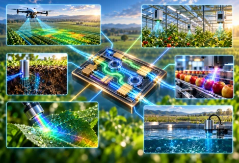
Having reached an acceptable level of maturity, PICs operating in the near infrared (NIR) are now being fielded in advanced telecommunications and information systems, as well as other applications including health care and agriculture [47]. Although some of these applications involve chemical sensing, MWIR spectroscopy that probes the strongest fingerprint absorption lines (rather than overtones) will ultimately provide orders of magnitude higher sensitivity. However, ultra-compact sensing PICs that integrate single-mode MWIR sources, detectors, passive sensing waveguides, and other optoelectronic components on the same chip must first bridge a substantial maturity gap. MWIR PICs are also needed for free space optical communication at wavelengths with more reliable atmospheric transmission, as well as a variety of systems for defense and security applications.
Quantum cascade lasers (QCLs) emitting at l = 4.8 µm [48] and interband cascade lasers (ICLs) [49] emitting at l = 3.6 µm [50] were successfully integrated on silicon in 2016 and 2018, respectively. MWIR high-speed E-O modulators [51], arrayed waveguide gratings (AWGs) for on-chip beam multiplexing and demultiplexing [52], on-chip supercontinuum generators [53], ring resonators [54], low-loss plasmonic waveguides [55], and membrane waveguides [56] have subsequently been demonstrated, and integrated QCLs have displayed functionality yield up to 98% [57]. Furthermore, QCLs and quantum cascade detectors (QCDs) processed from the same III-V QCL structure have been integrated [58], as have ICLs and interband cascade detectors (ICDs) [59]. ICLs have also been integrated with Chalcogenide glass waveguides, demonstrating a back-end compatible integration process. [60]
While QCLs and ICLs integrated on silicon have displayed relatively high performance, the realization of manufacturable high-sensitivity MWIR chemical sensing PICs has been delayed primarily by two factors:
(1) Very inefficient coupling between the III-V/silicon waveguides in which laser gain and/or photon detection are implemented, and passive waveguides that may provide propagation to other optoelectronic components on the PIC or provide a platform for sensing an analyte that may or may not be present in an ambient gas or liquid. The coupling inefficiency is due in part to a large vertical mismatch of the optical-mode profiles in the active and passive waveguides, which does not occur in NIR PICs. Architectural changes to the waveguides, e.g. as in reference [61], will mitigate the transfer efficiency, although these have not yet been reduced to practice.
(2) Immaturity of the waveguide architectures designed to maximize coupling between optical beams generated on the chip and gases or liquids of interest that are ambient to the chip. Besides weak evanescent coupling to ambient of the beam propagating in a conventional passive waveguide with relatively high core refractive index, the maximum sensing pathlength attainable on a compact chip is limited. Although implementations remain immature, the effective interaction length can be augmented, for example, by employing a cavity or ring resonator, processing a metamaterial surface on the sensing waveguide, or introducing a membrane sensing waveguide.
Nonetheless, we see no fundamental obstacles to overcoming these limitations, or to maximizing the performance of lasers, detectors, and other integrated MWIR components. In this context, we envision the following timeline for development of high-performance MWIR PICs that are manufacturable and affordable, as reflected in the Purple Brick Wall chart for Chem-sensors:
5 years – (a) Demonstration of efficient on-chip coupling between active and passive MWIR waveguides, to allow optical manipulation such as routing, beam splitting, spectral beam combining, etc.; (b) Proof-of-concept demonstration of on-chip MWIR spectroscopic sensing with ppm sensitivity.
10 years – (a) Maturation of prototype systems that integrate efficient waveguide architectures (footprint, low loss, high manufacturing yield, improved coupling efficiency between source-sensor-detector components) with sensitive chemical detection architectures; (b) Prototype packaging suitable for inexpensive mass production; (c) Proof-of-concept demonstration of on-chip MWIR spectroscopic sensing with ppb sensitivity; (d) Development of prototype MWIR PICs for defense and security applications.
15 years – Production and commercialization of packaged on-chip sensing systems that simultaneously manufacture hundreds or thousands of sensors on a single chip.
20 years – Commercial production of MWIR PICs that provide more specialized capabilities such as: (a) Multi-spectral sources and detectors on the same chip for multi-species sensing; (b) Broadband single-mode spectral tuning for sensing analytes such as organic molecules and explosives that have broad fingerprint features; (c) Remotely-positioned systems that broadcast sensing data and may run for years with little or no maintenance; (d) Solar-powered sensing systems, (e) Sensing systems for space platforms; (f) Systems designed for operation under harsh gaseous or liquid environments; (g) Systems designed for in vivo medical sensing.
Current QCLs-on-chip can be designed as sources integrated with spectrometers, with a monolithically integrated QCL array for spectroscopic applications already produced by various research teams. The narrow-distributed Bragg reflector in them is used for narrow-spectral emission for beam combining and tuning laser lines [62], [63,64,65],
Along with Chalcogenides and Ge, other platforms in the MWIR wavelength range are silver halide fibers and waveguides, III-V materials (InP, GaSb) that are used in manufacturing QCLs and QCDs, and Si/III-V platforms, achieved by heteroepitaxial growth. There is a common belief that MWIR technology is not ready for scalability. However, there are many manufacturers and volume producers of III-V structures for lasers, detectors, and platforms.
Some aspects of III-V MWIR technology are ready for scaling and mass-manufacturing. However, the early stage of the market remains a bottleneck to the high-volume manufacturing of MWIR components and related technologies [66]. Specifically, a need for: (1) a “killer application” (non-invasive glucose measurement and pervasive methane sensing are possible candidates) that would justify scaling; and (2) lower costs associated with high-volume manufacturing.
Although QCLs and ICLs are now incorporated into several commercial chemical sensing systems [67,68], most orders to foundries are currently for a small number of lasers defined by a certain specification, e.g., for use in academic research. On the other hand, a typical wafer grown by the foundry can provide about 1000 lasers (assuming a 3” InP wafer with 100% yield), and 6-8 wafers are typically grown at a time. Larger wafers (4”, 6”) and more extensive multiple growths would also be possible if the demand required it, but the multi-wafer reactors are currently under-used and the technology remains expensive.
Although QCLs provide excellent optical power and wavelength tunability, and miniaturized laser chips can be mass produced, the overall size of a complete QCL system (including power supplies, etc. and not just the chip itself) can be too bulky for applications where compactness is critical, such as handheld devices, wearables, or space applications. An ICL system can be somewhat smaller because drive power and thermal dissipation requirements are reduced by more than an order of magnitude.62a While thermal emitters and IR LEDs provide a broadband spectrum, which can be narrowed by filters or implementation in a resonant cavity, the light intensity is low and coupling to fiber or waveguide can be inefficient. There is also a need for MWIR detectors operating at room temperature with adequate sensitivity and low noise.
This topic is covered at length in other chapters. Table 3 outlines some general methods of integrating the passive and active PIC device components required for PIC sensors on SOI and InP platforms. Although monolithically integrated readout-integrated-circuits (ROICs) have been demonstrated and offer distinct performance advantages, they can be costly due to process incompatibility. 3D stacking methods using interposers should therefore be considered.
| Foundries/Com | Availability | Integration method | Photonic Process | Wavelength | Waveguide loss | Coupler loss | Device example | References |
| IMEC | Prototyping/ Research | Wire-Bond | 220nm SOI | 1550 nm | 1dB/cm | 2dB | Ring Resonator | 69,70 |
| Hewlett Packard | Prototyping/ Research | Wire-Bond | 130nm SOI | 1550 nm | 3dB/cm | 5dB | Ring Resonator | 71,72 |
| Luxtera/TSMC | High Volume/Bulk Manufac. | 3D Cu-pillar | 130nm SOI | 1310 nm | 1.9dB/cm | 2.2dB | MZM | 73 |
| ST Microelectronics | High Volume/Bulk Manufact | 3D Cu-pillar | PIC25G SOI | 1310 nm | 3dB/cm | 2.5dB | MZM | 74,75 |
| Luxtera | Medium Volume | N/A | 130nm SOI | 1550 nm | 1dB/cm | 1.5dB | MZM | 76 |
| IBM | High Volume | N/A | 90nm SOI | 1310 nm | 2.5dB/cm | 2.5dB | MZM | 77 |
| IHP | Medium Volume | N/A | 250nm BiCMOS | 1550 nm | 2.4dB/cm | 1.5dB | MZM | 78 |
| Oracle | Medium Volume | N/A | 130 nm SOI | 1550 nm | 3.5dB/cm | 5.5dB | Ring Resonator | 79 |
| Jeppix-Fraunhofer HHI | Medium Volume | N/A | InP | N/A | 2dB//cm loss | Thermo-optic Phase Modulator | 80 | |
| Jeppix-Smart Photonics | Medium Volume | N/A | InP | N/A | N/A | 2dB | MZI | 80 |
| Jeppix- | Medium Volume | N/A | InP | N/A | N/A | 4dB | MZI | 80 |
| Fraunhofer HHI | Prototyping/ Research | N/A | InP | N/A | <2dB/cm | 0.5dB | 81 | |
| Jeppix-Smart photonics | Medium Volume | N/A | InP | N/A | <2dB/cm | N/A | Lasers and Amplifiers | 80 |
| Max-IR Labs | N/A | N/A | N/A | N/A | N/A | N/A | QCL | 82,83 |
| Cornerstone | Prototyping/ Research | N/A | 220, 320, 500 nm SOI | 1550 nm | <3dB/cm (220); <0.8 dB/cm (340 | 5-6 dB (grating) | 84 |
Since the sensors require access to external environments, and in some cases also need functional coatings for capturing target analytes being sensed, packaging requirements for sensors are significantly different from other photonic integrated circuit (PIC) devices. These issues are discussed in the following subsections.
Waveguide coatings, as seen in Table 4, are an essential part of the sensor fabrication process. For spectroscopic sensing, these may be sorbent polymers or metal-organic frameworks (MOFs) intended to semi-selectively concentrate target analytes close to the waveguide. For biological, refractive index-based sensing, nucleic acids (DNA, RNA; this includes structured nucleic acids such as aptamers) and antibodies, among others, are typically attached to waveguides to capture target biomolecules with high specificity.
Oxide coatings are included because functionalization schemes often involve first deposition of an oxide-reactive silane. Control of the surface oxide thickness is essential given the exponential decay of the evanescent field. This is a well-controlled process for silicon and silicon nitride.
Deposition of reactive silanes has been demonstrated both at chip scale and wafer scale on silicon and silicon nitride. Limited work has been done on chip-scale silanization of alumina or aluminum [85]. Many silanes are available commercially.
Wafer-scale deposition of sorbent polymers is currently feasible, but only if the entire wafer is coated with a single polymer. Development opportunities in this area include methods for rapid wafer-scale ink jetting of sorbents (top-down), or other methods enabling deposition of multiple different kinds of sorbents on different areas of individual PICs at wafer scale. Likewise, biomaterials are currently attached to PICs using a “top-down” process, such as inkjet printing. While wafer-scale oligonucleotide synthesis was demonstrated as early as 1991 [86], and its commercialization was a driving force in the growth of the DNA microarray market at that time, equivalent technologies are not available for proteins and peptides. Additionally, although there is an existing industry focused on production of DNA sequences and antibodies for selective capture of biomolecules, development of sorbent polymers for selective capture of gaseous analytes or small-molecule biological analytes is at a very early stage.
Because biomolecules may be thermally sensitive (proteins and antibodies in particular rapidly denature when heated), the thermal budget for post-deposition processes must be extremely low. This highlights another development need in packaging.
Coatings for IR sensing can be used for:
Coupling light to and from fibers/waveguides is extremely important for practical applications and for enabling adoption in the industry. Active alignment is time consuming and expensive. There is a need for simple, rapid, and low-cost alignment techniques suitable for high throughput manufacturing. For refractive index-based sensing, grating couplers represent one viable solution to this, as these devices are less dependent on high-efficiency coupling than spectroscopic sensors. For spectroscopy, edge couplers for broadband light transmission exist, but high-efficiency grating couplers, grating couplers operating in TM mode, and effective polarization rotators are important development needs.
Many platforms are designed to operate at a single wavelength in the IR, however normally more than one wavelength measurement is needed to avoid cross-sensitivity and to compensate for drifts.
The limited selection of IR fibers consists mainly of: chalcogenide, fluoride, silver halides and hollow fibers. Since these fibers are also lossy, new fiber materials are needed to expand the applications of IR spectroscopy.
If feasible, an attractive alternative may be to integrate one or more semiconductor light sources and/or detectors on the same chip as the sensor.
It is important to distinguish between disposable and non-disposable sensors as far as I/O coupling is concerned. Disposable sensors must be cost-effective enough to compete with other sensors such as electrochemical sensors, which are small, low-cost, sensitive, and selective. This may not be compatible with fiber attach given current through-put levels.
For non-disposable sensors with long operational life, optical sensing and IR spectroscopy can have benefits, with direct sensing of a target analyte obviating the need to monitor indirect chemical reactions. The result is rapid and enables robust sensing. These can accommodate the added costs of fiber-attach.
Chemical and biological sensors require means for transporting the analyte sample (whether gas-phase or aqueous) to the sensing element. In many cases, concentration of the analyte (for example, enriching targets in an atmospheric sample) or processing (such as fractionation of a blood sample) are required. Many microfluidic strategies have been demonstrated, and some have been commercialized. Continued development is needed of methods for integrating PICs with microfluidics, and for packaging at scale. In the context of biosensors for medical diagnostics, passive microfluidic flow systems that are low-cost and disposable are of particular interest.
Microchip technology is now the pervasive solution across functions ranging from communication to computation to sensing and imaging, for products ranging from washing machines to automobiles to mega-data centers. Transistor dimensional scaling has reduced energy consumption and increased speed and functionality, simultaneously. Buried in the drive to maintain performance scaling are the realizations that i) iterative technology change has become insufficient, and ii) supply chain sustainability, in terms of workforce quality, materials criticality and manufacturing effluent, has no scaling vector. Economic risk has never been so large and rarely so dependent on technology evolution. The end of transistor/chip scaling has introduced the beginning of chip/package scaling. The need of the hour is a formal industry/government/academic infrastructure that can deliver consensus policy recommendations, technology goals and timelines, and education and workforce development products throughout the electronic-photonic packaging supply chain, in the form of an industry-adopted roadmap across three vectors:
Early ESG Goals for companies [92]: (i) Set aggressive, measurable sustainability targets while optimizing the sourcing for materials and minimizing waste, (ii) focus on minimizing the strain on water supplies and equip plants with cleaner backup power sources, (iii) reduce transportation footprint and (iv) control the use of hazardous chemicals.
To learn how a foundry can encourage sustainability, consider the example of imec. The imec sustainable semiconductor technology and systems (SSTS) program uses a software platform, imec.netzero, which was developed in-house. It functions as a virtual fab to deliver a quantified bottom-up view of IC manufacturing for various technologies, including future ones. Imec.netzero can act as a standard to estimate energy consumption, water usage, mineral usage, and greenhouse gas emissions associated with the fabrication of present and future logic CMOS technologies. Soon after imec presented results at the end of 2020 (which formed the basis of the program), it quickly grew to include equipment and material suppliers plus system and fabless players. Leading industry partners
and semiconductor organizations have begun to build sustainability goals and are holding their members accountable to sustainability standards like the Paris Accord.
While information needs to be gathered more broadly to understand global education and workforce needs, a survey of over 50 photonics firms in the US suggests that 2200 photonics jobs will be created annually, and current educational resources and student interest are insufficient to meet this growing demand [93]. Research universities, 4-year colleges, and community colleges gather to educate students and incumbent company employees in STEM topics through online courses, summer academies, hands-on bootcamps and workshops. Several companies have been involved in incentivizing STEM-skilling by offering well-paid summer internships and/or full-time jobs immediately after graduation. Key findings from an industry survey [94] led by Dr. Kirchain at MIT were (i) Photonics PhDs need more cross-training and training in Design for Manufacturing (DfM) and supply chain analysis; and (ii) Photonics technicians need to learn how to fabricate and assemble optical systems, diagnose and resolve process or product problems, design and execute testing, and recommend design changes. Sensor companies are a microcosm of the photonics industry and face similar challenges of being unable to find qualified workers.
Another example is from the Netherlands. PhotonDelta and Optics Netherlands have launched a first-of-its-kind ‘MasterPlus Programme in Optics and Photonics’ – in partnership with the Netherlands’ three leading technical universities: Delft University of Technology (TU Delft), Eindhoven University of Technology (TU/e), and University of Twente (UT).
The program will be a talent pipeline for the optics and photonics industry, which makes a significant contribution to the Dutch economy, and has a strong annual growth rate. By integrating academic expertise with industry needs, the program promises to produce highly skilled professionals poised to drive innovation and growth in the field.
One of the key barriers to rapid development in sensor manufacturing is the lack of broadly accepted standards. Although standards may arise organically from an understanding of materials and processes that produce the best performance (i.e. WG heights that enhance sensitivity), the process can be accelerated by targeting the three key areas below:
[1] Driesen-Worhoff, K.; Klein, E.; Hussein, G.; Driessen, A. “Silicon oxynitride based photonics” In: Proceedings of the IEEE 10th Anniversary International Conference on Transparent Optical Networks, Athens, Greece, 22–26 June 2008; Volume 3, pp. 266–269.
[2] Lo-Huang, Y.; Song, J.; Luo, X.; Liow, T. Y.; Lo, G. Q. “CMOS compatible monolithic multi-layer Si3N4 -on-SOI platform for low-loss high performance silicon photonics dense integration” Opt. Express 2014, 22, 21859–21865.
[3] Bauters, J. F.; Heck, M. J. R.; John, D.; Dai, D.; Tien, M. C.; Barton, J. S.; Leinse, A.; Heideman, R. G.; Blumenthal, D. J.; Bowers, J. E. “Ultra-low-loss high-aspect-ratio Si3N4 waveguides” Opt. Express 2011, 19, 3163–3174.
[4] Luke, K.; Dutt, A.; Poitras, C. B.; Lipson, M. “Overcoming Si3N4 film stress limitations for high quality factor ring resonators” Opt. Express 2013, 21, 22829–22833.
[5] Epping, J. P.; Hoekman, M.; Mateman, R.; Leinse, A.; Heideman, R. G.; van Rees, A.; van der Slot, P. J. M.; Lee, C. J.; Boller, K. J. “High confinement, high yield Si3N4 waveguides for nonlinear optical applications” Opt. Express 2015, 23, 642–648.
[6] Melchiorri, M.; Daldosso, N.; Sbrana, F.; Pavesi, L.; Pucker, G.; Kompocholis, C.; Bellutti, P.; Lui, A. “Propagation losses of silicon nitride waveguides in the near-infrared range” Appl. Phys. Lett. 2005, 86, 121111.
[7] Lo-Huang, Y.; Song, J.; Luo, X.; Liow, T. Y.; Lo, G. Q. “CMOS compatible monolithic multi-layer Si3N4 -on-SOI platform for low-loss high performance silicon photonics dense integration” Opt. Express 2014, 22, 21859–21865.
[8] Melchiorri, M.; Daldosso, N.; Sbrana, F.; Pavesi, L.; Pucker, G.; Kompocholis, C.; Bellutti, P.; Lui, A. “Propagation losses of silicon nitride waveguides in the near-infrared range” Appl. Phys. Lett. 2005, 86, 121111.
[9] Yoo-Shang, K.; Pathak, S.; Guan, B.; Liu, G.; Yoo, S. J. B. “Low-loss compact multilayer silicon nitride platform for 3D photonic integrated circuits” Opt. Express 2015, 23, 21334–21342.
[10] Ligentec-Pfeiffer, M. H. P.; Kordts, A.; Brasch, V.; Zervas, M.; Geiselmann, M.; Jost, J. D.; Kippenberg, T. J. “Photonic Damascene process for integrated high-Q microresonator based nonlinear photonics” Optica 2016, 3, 20–25.
[11] Chalmers-Krückel, C. J.; Fülöp, A.; Klintberg, T.; Bengtsson, J.; Andrekson, P. A.; Torres-Company, V. “Linear and nonlinear characterization of low-stress high-confinement silicon-rich nitride waveguides” Opt. Express 2015, 23, 25827–25837.
[12] Subramanian, A. Z.; Neutens, P.; Dhakal, A.; Jansen, R.; Claes, T.; Rottenberg, X.; Peyskens, F.; Selvaraja, S.; Helin, P.; Du Bois, B.; et al. “Low-Loss Singlemode PECVD Silicon Nitride Photonic Wire Waveguides for 532–900 nm Wavelength Window Fabricated Within a CMOS Pilot Line” IEEE Photonics J. 2013, 5, 2202809-2202809.
[13] Witzen-Romero-García, S.; Merget, F.; Zhong, F.; Finkelstein, H.; Witzens, J. “Silicon nitride CMOS-compatible platform for integrated photonics applications at visible wavelengths” Opt. Express 2013, 21, 14036–14046.
[14] Lo-Mao, S. C.; Tao, S. H.; Xu, Y. L.; Sun, X. W.; Yu, M. B.; Lo, G. Q.; Kwong, D. L. “Low propagation loss SiN optical waveguide prepared by optimal low-hydrogen module” Opt. Express 2008, 16, 20809–20816.
[16] Tyndall, N. F.; Stievater, T. H.; Kozak, D. A.; Pruessner, M. W.; Rabinovich, W. S.; Fahrenkopf, N. M.; Antohe, A. O.; McComber, K. A. “A low-loss SiN photonic integrated circuit foundry platform for waveguide-enhanced Raman spectroscopy" Proc. SPIE 2021, 11690,116900B.
[17] Fedeli, J. -M.; Nicoletti, S. "Mid-Infrared (Mid-IR) Silicon-Based Photonics," Proc. IEEE, 2018, 106, 2302-2312.
[18] Lin, H.; Luo, Z.; Gu, T.; Kimerling, L. C., Wada, K.; Agarwal, A.; Hu, J. "Mid-infrared integrated photonics on silicon: a perspective" Nanophotonics, 2018, 7, 393-420.
[19] Su, P.; Han, Z.; Kita, D.; Becla, P.; Lin, H.; Deckoff-Jones, S.; Richardson, K.; Kimerling, L. C.; Hu, J.; Agarwal, A. “Monolithic on-chip mid-IR methane gas sensor with waveguide-integrated detector” Appl. Phys. Lett. 2019, 114, 051103.
[20] Baker, J. E.; Sriram, R.; Miller, B. L. “Recognition-mediated particle detection under microfluidic flow with waveguide-coupled 2D photonic crystals: towards integrated photonic virus detectors” Lab on a Chip 2017, 17, 1570-1577.
[21] Herrier, C.; Morel, N.; Dubereuil, R.; Liu, J.; Gautheron, B.; Laplantine, L.; Rousselle, T.; Livache, T. “Imaging a smell: from plasmonic-based device to an array of Mach-Zehnder interferometers” Proc. SPIE2022, 12145, 1214503.
[22] Coutard, J. G.; Brun, M.; Fournier, M.; et al. « Volume Fabrication of Quantum Cascade Lasers on 200 mm-CMOS pilot line” Sci. Rep. 2020, 10, 6185.
[23] Nicoletti, S.; et al. "Challenges in the Miniaturization of Mid-IR Sensors Fully Integrated on Si" 2019 Conference on Lasers and Electro-Optics Europe & European Quantum Electronics Conference (CLEO/Europe-EQEC), 2019, pp. 1-1.
[24] Torre, A. D., et al. "Broadband and Flat Mid-Infrared Supercontinuum Generation in a Varying Dispersion Waveguide for Parallel Gas Spectroscopy" 2022 Conference on Lasers and Electro-Optics (CLEO), San Jose, CA, USA, 2022, pp. 1-2.
[25] Sinobad, M., et al. "Mid-infrared octave spanning supercontinuum generation to 8.5 μm in silicon-germanium waveguides" Optica 2018, 5, 360-366.
[26] Favreau, J., et al. "Development of a SiGe Arrayed Waveguide Grating in the 2185-2285 cm-1 range" Proc. ECIO, 2017, https://www.ecio-conference.org/wp-content/uploads/2017/03/ECIO_2017_T2.2.pdf
[27] Luff, B. J.; Wilkinson, J. S.; Piehler, J.; Hollenbach, U.; Ingenhoff, J.; Fabricius, N. “Integrated Optical Mach-Zehnder Biosensor” Journal of Lightwave Technology 1998, 16, 583–592.
[28] Kita, D. M.; Miranda, B.; Favela, D.; Bono, D.; Michon, J.; Lin, H.; Gu, T.; Hu, J. Nature Commun. 2018, 9, 4405.
[29] Prieto, F.; Sepúlveda, B.; Calle, A.; Liobera, A.; Dominguez, C.; Abad, A.; Montoya, A.; Lechuga, L. M. “An integrated optical interferometric nanodevice based on silicon technology for biosensor applications” Nanotechnology 2003, 14, 907.
[30] Luchansky, M. S.; Washburn, A. L.; McClellan, M. S.; Bailey, R. C. “Sensitive On-Chip Detection of a Protein Biomarker in Human Serum and Plasma over an Extended Dynamic Range Using Silicon Photonic Microring Resonators and Sub-Micron Beads” Lab Chip 2011, 11, 2042–2044.
[31] Cognetti, J. S.; Steiner, D. J.; Abedin, M.; Bryan, M. R.; Shanahan, C.; Tokranova, N.; Young, E.; Klose, A. M.; Zavriyev, A.; Judy, N.; Piorek, B.; Meinhart, C.; Jakubowicz, R.; Warren, H.; Cady, N. C.; Miller, B. L. “Disposable photonics for cost-effective clinical bioassays: application to COVID-19 antibody testing” Lab on a Chip, 2021, 21, 2913-2921.
[32] Mandel, S.; Erickson, D. “Nanoscale optofluidic sensor arrays” Opt. Express 2008, 16, 1623-1631.
[33] Baker, J. E.; Sriram, R.; Miller, B. L. Recognition-Mediated Particle Detection under Microfluidic Flow with Waveguide-Coupled 2D Photonic Crystals: Towards Integrated Photonic Virus Detectors. Lab Chip 2017, 17 (9), 1570–1577.
[34] Chakravarty, S.; Zou, Y.; Lai, W.-C.; Chen, R. T. “Slow light engineering for high Q high sensitivity photonic crystal microcavity biosensors in silicon” Biosens. Bioelectron. 2012, 38, 170-176.
[35] Armani, A. M.; Vahala, K. J. “Heavy water detection using ultra-high-Q microcavities” Opt. Lett. 2006, 31, 1896-1898.
[36] Bryan, M. R.; Butt, J. N.; Bucukovski, J.; Miller, B. L. “Biosensing with silicon nitride microring resonators integrated with on-chip filter bank spectrometry”, ACS Sensors, 2023, 8, 739-747.
[37] Zhou, J.; Husseini, D. A.; Li, J.; Lin, Z.; Sukhishvili, S.; Coté, G. L.; Gutierrez-Osuna, R.; Lin, P. T. “Mid-Infrared Serial Microring Resonator Array for Real-Time Detection of Vapor-Phase Volatile Organic Compounds” Anal. Chem. 2022, 94 (31), 11008–11015. https://doi.org/10.1021/acs.analchem.2c01463.
[38] Takahashi, H.; Suzuki, S.; Kato, K.; Nishi, I. “Arrayed-Waveguide Grating for Wavelength Division Multi/Demultiplexer with Nanometre Resolution” Electronics Letters 1990, 26, 87–88.
[39] Zhang, Z.; Wang, Y.; Tsang, H. K. “Tandem Configuration of Microrings and Arrayed Waveguide Gratings for a High-Resolution and Broadband Stationary Optical Spectrometer at 860 nm” ACS Photonics 2021, 8, 1251–1257.
[40] Ma, K.; Chen, K.; Zhu, N.; Liu, L.; He, S. “High-Resolution Compact On-Chip Spectrometer Based on an Echelle Grating With Densely Packed Waveguide Array” IEEE Photonics Journal 2019, 11, 1–7.
[41] P. Su , Z. Han, D. Kita , P. Becla, H. Lin , S. Deckoff-Jones, K. Richardson, L. C. Kimerling, J. Hu, and A. Agarwal, “Monolithic on-chip mid-IR methane gas sensor with waveguide-integrated detector”, Appl. Phys. Lett. 114, 051103 (2019); https://doi.org/10.1063/1.5053599
[42] Claes, T.; Bogaerts, W.; Bienstman, P. “Vernier-cascade label-free biosensor with integrated arrayed waveguide grating for wavelength interrogation with low-cost broadband source” Opt. Lett. 2011, 36, 3320-3322.
[43] Lo, S. M.; Hu, S.; Gaur, G.; Kostoulas, Y.; Weiss, S. M.; Fauchet, P. M. “Photonic crystal microring resonator for label-free biosensing” Opt. Express 2017, 25, 7046-7054.
[44] Tyndall, N. F.; Kozak, D. A.; Pruessner, M. W.; Goetz, P. G.; Rabinovich, W. S.; Stievater, T. H.; Bryan, M. R.; Luta, E.; Miller, B. L.; Fahrenkopf, N. M.; Antohe, A. “Low-loss nanoslot waveguides for sensing fabricated in a CMOS foundry” CLEO: Sci. Innov. 2021, 2021, Stu1A.7.
[45] Barrios, C. A. “Optical slot-waveguide based biochemical sensors” Sensors 2009, 9, 4751-4765.
[46] https://www.aimphotonics.com/pdk
[47] De Vries, C. “PICs set their sights beyond data and telecom” Photonics Spectra, January 2023, 104.
[48] Spott, A.; Peters, J. D.; Davenport, M. L.; Stanton, E. J.; Merritt, C. D.; Bewley, W. W.; Vurgaftman, I.; Kim, C. S.; Meyer, J. R.; Kirch, J. D.; Mawst, L. J.; Botez, D.; Bowers, J. E. “Quatum cascade laser on silicon” Optica 2016, 3, 545.
[49] J. R. Meyer, W. W. Bewley, C. L. Canedy, C. S. Kim, M. Kim, C. D. Merritt, and I. Vurgaftman, “The Interband Cascade Laser,” Photonics 7, 75 (2020).
[50] Spott, A.; Stanton, E. J.; Torres, A.; Davenport, M. L.; Canedy, C. L.; Vurgaftman, I.; Kim, M.; Kim, C. S.; Merritt, C. D.; Bewley, W. W.; Meyer, J. R.; Bowers, J. E. “Interband cascade laser on silicon” Optica, 2018, 5, 996.
[51] Montesinos-Ballester, M; Deniel, L.; Koompai, N.; Nguyen, T. H. N.; Frigerio, J.; Ballabio, A.; Falcone, V.; Le Roux, X.; Alonso-Ramos, C.; Vivien, L.; Bousseksou, A.; Isella, G.; Marris-Morini, D. “Mid-infrared Integrated Electro-optic Modulator Operating up to 225 MHz between 6.4 and 10.7 μm Wavelength” ACS Phot. 2022, 9, 249-255.
[52] Malik, A.; Spott, A.; Stanton, E. J.; Peters, J. D.; Mawst, L. J.; Botez, D.; Meyer, J. R.; Bowers, J. E. “Integration of Mid-Infrared Light Sources on Silicon Based Waveguide Platforms in 3.5 – 4.7 µm Wavelength Range.” IEEE J. Sel. Topics Quant. Electron. 2019, 25, 1502809.
[53] Della Torre, A.; Armand, R.; Sinobad, M.; Fiaboe, K. F.; Luther-Davies, B.; Madden, S. J.; Mitchell, A.; Nguyen, T.; Moss, D. J.; Hartmann, J.-M.; Reboud, V.; Fédéli, J.-M.; Monat, C.; Grillet, C. IEEE J. Sel. Topics Quant. Electron. 2023, 29, 5100509.
[54] Kozak, D. A.; Tyndall, N. F.; Pruessner, M. W.; Rabinovich, W. S.; Stievater, T. H. “Germanium-on-silicon waveguides for long-wave integrated photonics: ring resonance and thermo-optics” Opt. Expr. 2021, 29, 15443.
[55] David, M.; Dabrowska, A.; Sistani, M.; Doganlar, I. C.; Hinkelmann, E.; Detz, H.; Weber, W. M.; Lendl, B.; Strasser, G.; Hinkov, B. “Octave-spanning low-loss mid-IR waveguides based on semiconductor-loaded plasmonic” Opt. Expr. 2021, 29, 43567.
[56] Vik, M.; Datta, A.; Alberti, S.; Yallew, H. D.; Mittal, V.; Murugan, G. S.; Jágerská, J. “Extraordinary evanescent field confinement waveguide sensor for mid-infrared trace gas spectroscopy” Light: Sci. & Appl. 2021, 10, 26.
[57] Coutard, J. G.; Brun, M.; Fournier, M.; Lartigue, O.; Fedeli, F.; Maisons, G.; Fedeli, J. M.; Nicoletti, S.; Carras, M.; Duraffourg, L. “Volume Fabrication of Quantum Cascade Lasers on 200 mm-CMOS pilot line” Sci. Rep. 2020, 10, 6185.
[58] B. Schwarz, P. Feininger, H. Detz, T. Zederbauer, A. M. Andrews, S. Kalchmair, W. Schrenk, O. Baumgartner, H. Kosina, and G. Strasser, Appl. Phys. Lett. 101, 191109 (2012), “A bi-functional quantum cascade device for same-frequency lasing and detection.”
[59] H. Lotfi, L. Li, S. M. S. Rassel, R. Q. Yang, C. J. Correege, M. B. Johnson, P. R. Larson, J. A. Gupta, Appl. Phys. Lett. 109, 151111 (2016), “Monolithically integrated mid-IR interband cascade laser and photodetector operating at room temperature.”
[60] H. Lin, C. S. Kim, L. Li, M. Kim, W. W. Bewley, C. D. Merritt, C. L. Canedy, I. Vurgaftman, A. Agarwal, K. Richardson, J. Hu, and J. R. Meyer, “Monolithic Chalcogenide Glass Waveguide Integrated Interband Cascaded Laser,” Opt. Mat. Expr. 11, 2869 (2021).
[61] J. R. Meyer, A. Spott, C. S. Kim, M. Kim, C. L. Canedy, C. D. Merritt, W. W. Bewley, and I. Vurgaftman, U.S. Patent Application 18/149,778 filed 4 January 2023, “Weak Index Guiding of Interband Cascade Lasers.”
[62] A. Lyakh et al., High peak power quantum cascade laser arrays with top-metal distributed Brag Reflector, SPIE PC12372 (2023)
[63] K. Zhang et al., “mid-infrared photonic integration on InP”, Conf. Proc. Novel in-plane Semiconductor Lasers XXII, C124400K (SPIE)
[64] Hinkov et al, Real-time monitoring of liquids on the chip-scale (2022)
[65] B. Schwartz et al., Monolithically integrated mid-infrared lab-on-a-chip iusing plasminics and quantum cascade structures, Nature Communications 5, 4085 (2014)
[66] M. Troccoli, “Can QCLs have a strong impact on health and environmental applications”, SPIE PC12372
[67] www.marketsandmarkets.com/Market-Reports/quantum-cascade-laser-market-163177255.html
[68] www.nanoplus.com/products/interband-cascade-laser
[69] M. Pantouvaki, P. De Heyn, R. Michal, P. Verheyen, S. Brad, A. Srinivasan, H. Chen, J. De Coster, G. Lepage, P. Absil, and J. Van Campenhout, “50Gb/s Silicon Photonics Platform for Short-Reach Optical Interconnects,” in Optical Fiber Communication Conference, OSA Technical Digest (online) (Optical Society of America, 2016), paper Th4H.4.
[70] M. Rakowski, M. Pantouvaki, P. Verheyen, J. De Coster, G. Lepage, P. Absil, and J. Van Campenhout, “A 50Gb/s, 610fJ/bit hybrid CMOS-Si photonics ring-based NRZ-OOK transmitter,” in Optical Fiber Communications Conference, OSA Technical Digest (online) (Optical Society of America, 2016), pp. 1–3.
[71] K. Yu, C. Li, H. Li, A. Titriku, A. Shafik, B. Wang, Z. Wang, R. Bai, C. H. Chen, M. Fiorentino, P. Y. Chiang, and S. Palermo, “A 25 Gb/s Hybrid-Integrated Silicon Photonic Source-Synchronous Receiver With Microring Wavelength Stabilization,” IEEE Journal of Solid-State Circuits 51(9), 2129–2141 (2016).
[72] H. Li, Z. Xuan, A. Titriku, C. Li, K. Yu, B. Wang, A. Shafik, N. Qi, Y. Liu, R. Ding, T. Baehr-Jones, M. Fiorentino, M. Hochberg, S. Palermo, and P. Y. Chiang, “A 25 Gb/s, 4.4 V-Swing, AC-Coupled Ring Modulator-Based WDM Transmitter with Wavelength Stabilization in 65 nm CMOS,” IEEE Journal of Solid-State Circuits 50(12), 3145–3159 (2015)
[73] P. De Dobbelaere, A. Dahl, A. Mekis, B. Chase, B. Weber, B. Welch, D. Foltz, G. Armijo, G. Masini, G. McGee, G. Wong, J. Balardeta, J. Dotson, J. Schramm, K. Hon, K. Khauv, K. Robertson, K. Stechschulte, K. Yokoyama, L. Planchon, L. Tullgren, M. Eker, M. Mack, M. Peterson, N. Rudnick, P. Milton, P. Sun, R. Bruck, R. Zhou, S. Denton, S. Fathpour, S. Gloeckner, S. Jackson, S. Pang, S. Sahni, S. Wang, S. Yu, T. Pinguet, Y. De Koninck, Y. Chi, and Y. Liang, “Advanced Silicon Photonics Technology Platform Leveraging a Semiconductor Supply Chain,” in Proceedings of IEEE International Electron Devices Meeting (IEEE, 2017), paper 34.1.
[74] F. Boeuf, S. Cremer, N. Vulliet, T. Pinguet, A. Mekis, G. Masini, L. Verslegers, P. Sun, A. Ayazi, N. K. Hon, S. Sahn, Y. Chi, B. Orlando, D. Ristoiu, A. Farcy, F. Leverd, L. Broussous, D. Pelissier-Tanon, C. Richard, L. Pinzelli, R. Beneyton, O. Gourhant, E. Gourvest, Y. Le-Friec, D. Monnier, P. Brun, M. Guillermet, D. Benoit, K. Haxaire, J. R. Manouvrier, S. Jan, H. Petiton, J. F. Carpentier, T. Quemerais, C. Durand, D. Gloria, M. Fourel, F. Battegay, Y. Sanchez, E. Batail, F. Baron, P. Delpech, L. Salager, P. De Dobbelaere, and B. Sautreuil, “A multi-wavelength 3D-compatible silicon photonics platform on 300mm SOI wafers for 25Gb/s applications,” in Proceedings of IEEE International Electron Devices Meeting (IEEE, 2013), pp. 13.3.1–13.3.4.
[75] E. Temporiti, G. Minoia, M. Repossi, D. Baldi, A. Ghilioni, and F. Svelto, “A 56Gb/s 300mW silicon-photonics transmitter in 3D-integrated PIC25G and 55nm BiCMOS technologies,” in Proceedings of IEEE International Solid-State Circuits Conference, (IEEE, 2016), pp. 404–405.
[76] A. Narasimha, B. Analui, E. Balmater, A. Clark, T. Gal, D. Guckenberger, S. Gutierrez, M. Harrison, R. Ingram, R. Koumans, D. Kucharski, K. Leap, Y. Liang, A. Mekis, S. Mirsaidi, M. Peterson, T. Pham, T. Pinguet, D. Rines, V. Sadagopan, T. J. Sleboda, D. Song, Y. Wang, B. Welch, J. Witzens, S. Abdalla, S. Gloeckner, and P. De Dobbelaere, “A 40-Gb/s QSFP Optoelectronic Transceiver in a 0.13 µm CMOS Silicon-on-Insulator Technology,” in Optical Fiber Communication Conference, OSA Technical Digest (online) (Optical Society of America, 2008), pp. 1–3
[77] N. B. Feilchenfeld, F. G.,erson, T. Barwicz, S. Chilstedt, Y. Ding, J. Ellis-Monaghan, D. M. Gill, C. Hedges, J. Hofrichter, F. Horst, M. Khater, E. Kiewra, R. Leidy, Y. Martin, K. McLean, M. Nicewicz, J. S. Orcutt, B. Porth, J. Proesel, C. Reinholm, J. C. Rosenberg, W. D. Sacher, A. D. Stricker, C. Whiting, C. Xiong, A. Agrawal, F. Baker, C. W. Baks, B. Cucci, D. Dang, T. Doan, F. Doany, S. Engelmann, M. Gordon, E. Joseph, J. Maling, S. Shank, X. Tian, C. Willets, J. Ferrario, M. Meghelli, F. Libsch, B. Offrein, W. M. J. Green, W. Haensch, “An integrated silicon photonics technology for O-band datacom,” in Proceedings of IEEE International Electron Devices Meeting, (IEEE, 2015), pp. 25.7.1–25.7.4.
[78] L. Zimmermann, D. Knoll, M. Kroh, S. Lischke, D. Petousi, G. Winzer, and Y. Yamamoto, “BiCMOS Silicon Photonics Platform,” in Optical Fiber Communication Conference, OSA Technical Digest (online) (Optical Society of America, 2015), paper Th4E.5
[79] J. F. Buckwalter, X. Zheng, G. Li, K. Raj, and A. V. Krishnamoorthy, “A Monolithic 25-Gb/s Transceiver With Photonic Ring Modulators and Ge Detectors in a 130-nm CMOS SOI Process,” IEEE Journal of Solid-State Circuits 47(6), 1309–1322 (2012
[80] https://www.jeppix.eu/mpw-services/workflow/performance-summary-table/
[81] Fraunhofer HHI: https://www.hhi.fraunhofer.de/en/departments/pc/research-groups/photonic-inp-foundry/our-offer.html
[82] https://www.max-ir-labs.com/#Sensor
[83] https://www.spiedigitallibrary.org/conference-proceedings-of-spie/11233/112330C/Nitrogen-sensor-based-on-quantum-cascade-lasers-QCLs-for-wastewater/10.1117/12.2553691.short?SSO=1
[84] https://www.cornerstone.sotonfab.co.uk/our-services/
[85] Luta, E. P.; Miller, B. L. “Development of methods for specific capture of biological targets on aluminum substrates: application to Bacillus subtilis spore detection as a model for anthrax” Sensors, 2022, 22, 3441.
[86] https://pubmed.ncbi.nlm.nih.gov/1990438/
[87] Yadav, A. R.; Sriram, R.; Carter, J. A.; Miller, B. L. “Comparative study of solution phase and vapor phase deposition of aminosilanes on silicon dioxide surfaces”, Mat. Sci. Eng. C 2014, 35, 283-290.
[88] Tyndall, N.; Stievater, T. H.; Kozak, D.; Pruessner, M.; Roxworthy, B.; Rabinovich, W.; Roberts, C.; McGill, A.; Miller, B. L.; Luta, E.; Yates, M. “Figure-of-merit characterization of hydrogen-bond acidic sorbents for waveguide-enhanced Raman spectroscopy” ACS Sensors, 2020, 5, 831-836.
[89] https://pubmed.ncbi.nlm.nih.gov/33599039/
[90] https://www.science.org/cms/asset/a790a805-11b0-45c9-8610-9899f9961df3/pap.pdf
[91] Jana Jágerská, Firehun T. Dullo, Martin Ingvaldsen, Susan M. Lindecrantz, Magnus Engqvist, Jørn Hansen, and
Olav G. Hellesø, “On-Chip Methane Sensing with Cryptophane-A Cladded Waveguide Interferometers”, Conference on Lasers and Electro-Optics OSA Technical Digest (2016) (Optica Publishing Group, 2016), paper SF2H.3 https://doi.org/10.1364/CLEO_SI.2016.SF2H.3
[92] How semiconductor companies can lead on sustainability issues, by Englund, Eliadis, Flynn, Lubowe, Ernst & Young website: https://www.ey.com/en_us/tmt/how-semiconductor-companies-can-lead-on-sustainability
[95] https://www.microfluidic-chipshop.com
Join the working group and help shape the IPSR chapters.
Help us improve this section for the next reader.